Full Text Searchable PDF User Manual
September 2003
1/15
®
STV9302A
Vertical Deflection Booster
for 2-A
PP
TV/Monitor Applications with 70-V Flyback Generator
Main Features
■
Power Amplifier
■
Flyback Generator
■
Output Current up to 2 App
■
Thermal Protection
■
Stand-by Control
Description
The STV9302A is a vertical deflection booster
designed for TV and monitor applications.
This device, supplied with up to 35 V, provides up to
2 App output current to drive the vertical deflection
yoke.
The internal flyback generator delivers flyback
voltages up to 70 V.
in double-supply applications, a stand-by state will
be reached by stopping the (+) supply alone.
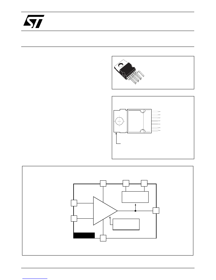
HEPTAWATT
(Plastic Package)
ORDER CODE: STV9302A
7
6
5
4
3
2
1
Tab connected
Input (Non Inverting)
Output Stage Supply
Output
Ground Or Negative Supply
Flyback Generator
Supply Voltage
Input (Inverting)
to pin 4
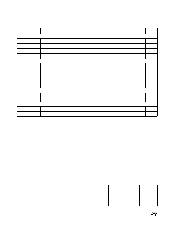
1
Thermal
Protection
6
4
3
5
STV9302A
+
-
Power
Amplifier
7
2
Flyback
Generator
Inverting
Non-Inverting
Input
Input
Ground or Negative Supply
Output
Flyback
Generator
Output Stage
Supply
Voltage
Supply
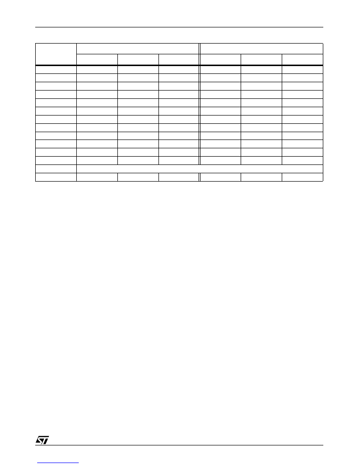
Absolute Maximum Ratings
STV9302A
2/15
1
Absolute Maximum Ratings
Note:1. Usually the flyback voltage is slightly more than 2 x V
S
. This must be taken into consideration when
setting
V
S.
2. Versus pin 4
3. V3 is higher than V
S
during the first half of the flyback pulse.
4. Such repetitive output peak currents are usually observed just before and after the flyback pulse.
5. This non-repetitive output peak current can be observed, for example, during the Switch-On/Switch-
Off phases. This peak current is acceptable providing the SOA is respected (
Figure 8
and
Figure 9
).
6. All pins have a reverse diode towards pin 4, these diodes should never be forward-biased.
7. Input voltages must not exceed the lower value of either V
S
+ 2 or 40 volts.
2
Thermal Data
Symbol
Parameter
Value
Unit
Voltage
V
S
Supply Voltage (pin 2) -
Note 1
and
Note 2
40
V
V
5
, V
6
Flyback Peak Voltage -
Note 2
70
V
V
3
Voltage at Pin 3 -
Note 2
,
Note 3
and
Note 6
-0.4 to (V
S
+ 3)
V
V
1
, V
7
Amplifier Input Voltage -
Note 2
,
Note 6
and
Note 7
- 0.4 to (V
S
+ 2) or +40
V
Current
I
0
(1)
Output Peak Current at f = 50 to 200 Hz, t
≤
10µs -
Note 4
±5
A
I
0
(2)
Output Peak Current non-repetitive -
Note 5
±2
A
I
3
Sink
Sink Current, t<1ms -
Note 3
1.5
A
I
3
Source
Source Current, t
<
1ms
1.5
A
I
3
Flyback pulse current at f=50 to 200 Hz, t
≤
10
µ
s -
Note 4
±5
A
ESD Susceptibility
ESD1
Human body model (100 pF discharged through 1.5 k
Ω
)
2
kV
ESD2
EIAJ Standard (200 pF discharged through 0
Ω
)
300
V
Temperature
T
s
Storage Temperature
-40 to 150
°C
T
j
Junction Temperature
+150
°C
Symbol
Parameter
Value
Unit
R
thJC
Junction-to-Case Thermal Resistance
3
°C/W
T
T
Temperature for Thermal Shutdown
150
°C
T
J
Recommended Max. Junction Temperature
120
°C
3/15
STV9302A
Electrical Characteristics
3
Electrical Characteristics
(V
S
= 32 V, T
AMB
= 25°C, unless otherwise specified)
8. In normal applications, the peak flyback voltage is slightly greater than 2 x (V
S
- V
4
). Therefore, (V
S
- V
4
) = 35 V is not allowed without special circuitry.
9. Refer to
Figure 4
, Stand-by condition.
Symbol
Parameter
Test Conditions
Min.
Typ.
Max.
Unit
Fig.
Supply
V
S
Operating Supply Voltage Range (V
2
-V
4
)
Note 8
10
35
V
I
2
Pin 2 Quiescent Current
I
3
= 0, I
5
= 0
5
20
mA
1
I
6
Pin 6 Quiescent Current
I
3
= 0, I
5
= 0, V
6
=35v
8
19
50
mA
1
Input
I
1
Input Bias Current
V
1
= 1 V, V
7
= 2.2 V
- 0.6
-1.5
µ
A
1
I
7
Input Bias Current
V
1
= 2.2 V, V
7
= 1 V
- 0.6
-1.5
µ
A
V
IR
Operating Input Voltage Range
0
V
S
- 2
V
V
I0
Offset Voltage
2
mV
∆
V
I0
/dt
Offset Drift versus Temperature
10
µ
V/°C
Output
I
0
Operating Peak Output Current
±1
A
V
5L
Output Saturation Voltage to pin 4
I
5
= 1 A
1
1.7
V
3
V
5H
Output Saturation Voltage to pin 6
I
5
= -1 A
1.8
2.3
V
2
Stand-by
V
5STBY
Output Voltage in Stand-by
V
1
= V
7
= V
S
= 0
See
Note 9
V
S
- 2
V
Miscellaneous
G
Voltage Gain
80
dB
V
D5-6
Diode Forward Voltage Between pins 5-6
I
5
= 1 A
1.4
2
V
V
D3-2
Diode Forward Voltage between pins 3-2
I
3
= 1 A
1.3
2
V
V
3SL
Saturation Voltage on pin 3
I
3
= 20 mA
0.4
1
V
3
V
3SH
Saturation Voltage to pin 2 (2nd part of flyback)
I
3
= -1 A
2.1
V
Electrical Characteristics
STV9302A
4/15
Figure 1: Measurement of I
1
, I
2
and I
6
Figure 2: Measurement of V
5H
Figure 3: Measurement of V
3L
and V
5L
1V
(a)
39k
Ω
5
1
(b)
I1
(a): I2 and I6 measurement
(b): I1 measurement
S
+Vs
2
6
I2
I6
4
7
2.2V
STV9302A
5.6k
Ω
- I5
5
1V
7
2.2V
1
4
+Vs
2
6
V
5H
STV9302A
+Vs
I3 or I5
3
5
V
5L
V
3L
(a)
(b)
(a): V
5L
measurement
(b): V
3L
measurement
STV9302A
1V
7
4
2
6
2.2V
1
5/15
STV9302A
Application Hints
4
Application Hints
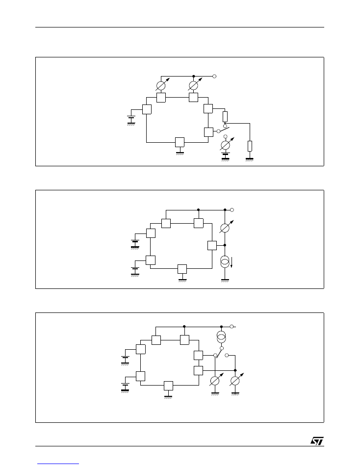
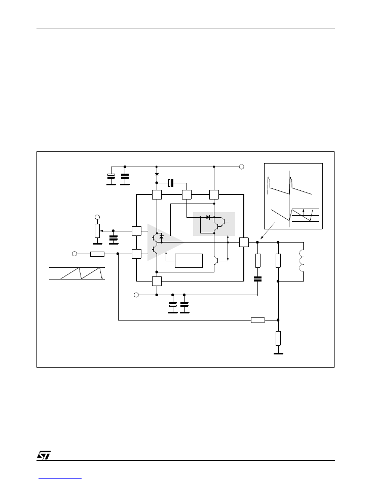
The yoke can be coupled either in AC or DC.
4.1
DC-coupled Application
When DC coupled (see
Figure 4
), the display vertical position can be adjusted with input bias. On
the other hand, 2 supply sources (V
S
and -V
EE
) are required.
A Stand-by state will be reached by switching OFF the positive supply alone. In this state, where
both inputs are the same voltage as pin 2 or higher, the output will sink negligible current from the
deviation coil.
4.1.1
Application Hints
For calculations, treat the IC as an op-amp, where the feedback loop maintains V
1
= V
7
.
Figure 4: DC-coupled Application
R3
+Vs
R2
R1
Rd(*)
Yoke
Ly
Vertical Position
Adjustment
-V
EE
Vref
(*) recommended:
Ly
50
µ
s
-------------
Rd
Ly
20
µ
s
-------------
<
<
0.1µF
0.1µF
C
F
(47 to 100µF)
Power
Amplifier
Flyback
Generator
Thermal
Safety
470µF
470µF
Output
Current
Output
Voltage
I
p
000000000000000000
00000000000000000
000000000000000000 000000000000000000
000000000000000000
000000000000000000
00000000000000000
00000000000000000
7
3
2
5
6
1
4
V
M
V
m
+
-
0
.22
µF
1.5
Ω
Application Hints
STV9302A
6/15
4.1.1.1 Centering
Display will be centered (null mean current in yoke) when voltage on pin 7 is (R
1
is negligible):
4.1.1.2 Peak Current
Example: for V
m
= 2 V, V
M
= 5 V and I
P
= 1 A
Choose R
1
in the1
Ω
range, for instance R
1
=1
Ω
From equation of peak current:
Then choose R
2
or R
3
. For instance, if R
2
= 10 k
Ω
, then R
3
= 15 k
Ω
Finally, the bias voltage on pin 7 should be:
4.1.2
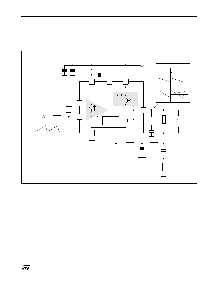
Ripple Rejection
When both ramp signal and bias are provided by the same driver IC, you can gain natural rejection
of any ripple caused by a voltage drop in the ground (see
Figure 5
), if you manage to apply the
same fraction of ripple voltage to both booster inputs. For that purpose, arrange an intermediate
point in the bias resistor bridge, such that (R
8
/ R
7
) = (R
3
/ R
2
), and connect the bias filtering
capacitor between the intermediate point and the local driver ground. Of course, R
7
should be
connected to the booster reference point, which is the ground side of R
1
.
Figure 5: Ripple Rejection
V
7
V
M
V
m
+
2
------------------------
R
2
R
2
R
3
+
----------------------
ÿ
þ
×
=
I
P
V
M
V
m
–
(
)
2
-----------------------------
R
2
R
1
xR
3
-------------------
×
=
R
2
R
3
-------
2
I
P
R
1
×
×
V
M
V
m
–
-----------------------------
2
3
---
=
=
V
7
V
M
V
m
+
2
------------------------
1
1
R
3
R
2
-------
+
-----------------
×
7
2
---
1
2.5
--------
×
1.4V
=
=
=
R
3
R
2
R
1
Rd
Yoke
Ly
Power
Amplifier
Flyback
Generator
Thermal
Safety
0000000000000000
0000000000000000
7
3
2
5
6
1
4
+
-
0000000000000000
0000000000000000
R
7
R
8
R
9
000000
000000
000000
Reference
Voltage
Ramp
Signal
Driver
Ground
Source of Ripple
7/15
STV9302A
Application Hints
4.2
AC-Coupled Applications
In AC-coupled applications (See
Figure 6
), only one supply (V
S
) is needed. The vertical position of
the scanning cannot be adjusted with input bias (for that purpose, usually some current is injected
or sunk with a resistor in the low side of the yoke).
4.2.1
Application Hints
Gain is defined as in the previous case:
Choose R
1
then either R
2
or R
3
. For good output centering, V
7
must fulfill the following equation:
or
Figure 6: AC-coupled Application
R
3
+Vs
R
2
R
1
Rd(*)
Yoke
Ly
(*)
recommended:
Ly
50
µ
s
-------------
Rd
Ly
20
µ
s
-------------
<
<
0.1µF
C
F
(47 to 100µF)
Power
Amplifier
Flyback
Generator
Thermal
Safety
470µF
Output
Current
Output
Voltage
I
p
000000000000000000
000000000000000000
000000000000000000
000000000000000000
000000000000000000
000000000000000000
7
3
2
5
6
1
4
V
M
V
m
+
-
000000000000000000
00000000000000000
00000000000000000
000000000000000000
000000000000000000
C
s
R
4
000000000000000000
C
L
R
5
0.22
µF
1.5
Ω
I
p
V
M
V
m
–
2
------------------------
R
2
R
1
R
3
×
----------------------
×
=
V
S
2
--------
V
7
–
R
4
R
5
+
----------------------
V
7
V
M
V
m
+
2
------------------------
–
R
3
--------------------------------------
V
7
R
2
-------
+
=
V
7
1
R
3
-------
ÿ
1
R
2
-------
+
×
1
R
4
R
5
+
----------------------
þ
V
S
2 R
4
R
5
+
(
)
------------------------------
V
M
V
m
+
2
R
3
×
------------------------
+
ÿ
þ
=
+
Application Hints
STV9302A
8/15
C
S
performs an integration of the parabolic signal on C
L
, therefore the amount of S correction is set
by the combination of C
L
and C
s
.
4.3
Application with Differential-output Drivers
Certain driver ICs provide the ramp signal in differential form, as two current sources i
+
and i
−
with
opposite variations.
Let us set some definitions:
●
i
cm
is the common-mode current:
●
at peak of signal, i
+
= i
cm
+ i
p
and i
−
= i
cm
- i
p
, therefore the peak differential signal is i
p
- (-
i
p
) = 2 i
p
, and the peak-peak differential signal, 4i
p
.
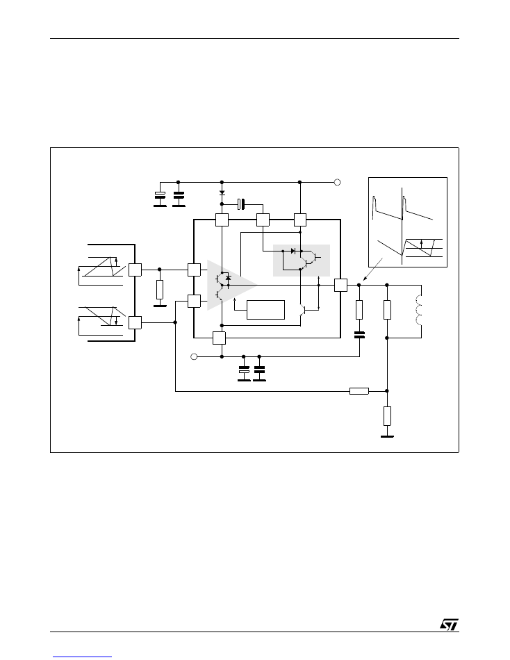
The application is described in
Figure 7
with DC yoke coupling. The calculations still rely on the fact
that V
1
remains equal to V
7
.
Figure 7: Using a Differential-output Driver
+Vs
R
2
R
1
Rd(*)
Yoke
Ly
-V
EE
0.
2
2µF
(*)
recommended:
Ly
50
µ
s
--------------
Rd
Ly
20
µ
s
--------------
<
<
0.1µF
0.1µF
C
F
(47 to 100µF)
Power
Amplifier
Flyback
Generator
Thermal
Safety
+
-
470µF
470µF
Output
Current
Output
Voltage
I
p
000000000000000000
000000000000000000
000000000000000000
000000000000000000
00000000000000000
00000000000000000
00000000000000000
00000000000000000
00000000000000000
00000000000000000
7
3
2
5
6
1
4
R
7
00000000000000000
00000000000000000
+
-
Differential output
driver IC
i
p
i
cm
-i
p
i
cm
1.5
Ω
i
cm
1
2
--- i
+
i
-
+
(
)
=
9/15
STV9302A
Application Hints
4.3.1
Centring
When idle, both driver outputs provide i
cm
and the yoke current should be null (R
1
is negligible),
hence:
4.3.2
Peak Current
Scanning current should be I
P
when positive and negative driver outputs provide respectively
i
cm
- i
p
and i
cm
+ i
p
, therefore
and since R
7
= R
2
:
Choose R
1
in the 1
Ω
range, the value of R
2
= R
7
follows. Remember that i is one-quarter of driver
peak-peak differential signal! Also check that the voltages on the driver outputs remain inside
allowed range.
●
Example: for i
cm
= 0.4mA, i = 0.2mA (corresponding to 0.8mA of peak-peak differential
current), I
p
= 1A
Choose R
1
= 0.75
Ω
, it follows R
2
= R
7
= 1.875k
Ω
.
4.3.3
Ripple Rejection
Make sure to connect R
7
directly to the ground side of R
1
.
4.3.4
Secondary Breakdown Diagrams
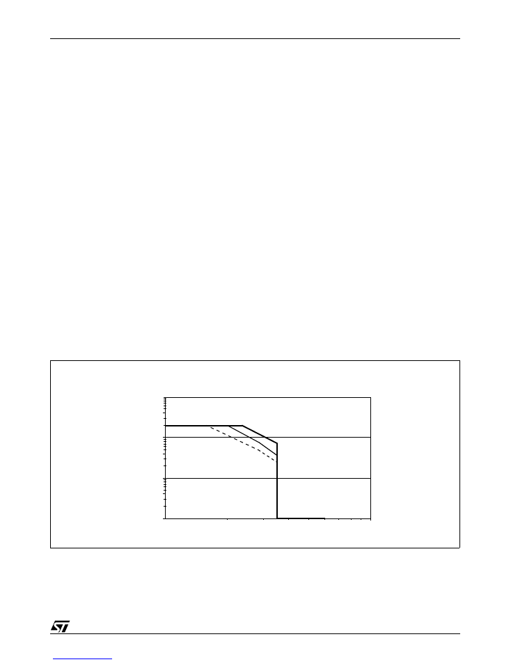
The diagram has been arbitrarily limited to max VS (35 V) and max I0 (2 A).
Figure 8: Output Transistor Safe Operating Area (SOA) for Secondary Breakdown
i
cm
R
7
⋅
i
cm
R
2
therefore R
7
R
2
=
⋅
=
i
cm
i
–
(
)
R
7
⋅
I
p
R
1
⋅
i
cm
i
+
(
)
R
2
⋅
+
=
I
p
i
-----
2R
7
R
1
-----------
–
=
100
µ
s
10ms
100ms
0.01
0.1
1
10
10
60
100
Volts
Ic
(A)
@ Tcase=25°C
35
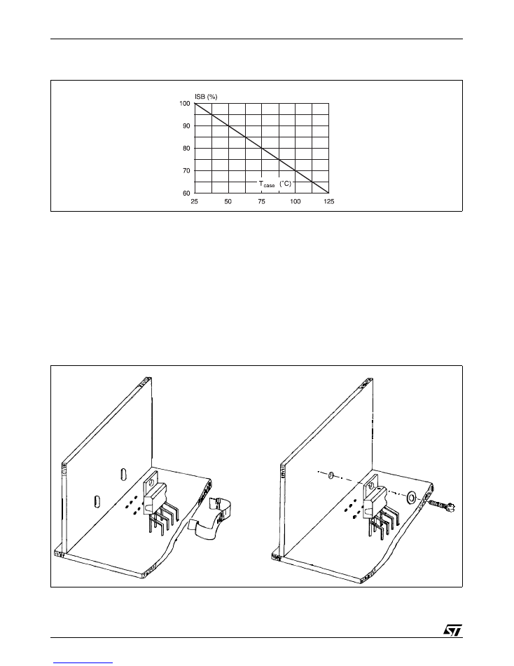
Mounting Instructions
STV9302A
10/15
5
Mounting Instructions
The power dissipated in the circuit is removed by adding an external heatsink. With the
HEPTAWATT
™
package, the heatsink is simply attached with a screw or a compression spring
(clip).
A layer of silicon grease inserted between heatsink and package optimizes thermal contact. In DC-
coupled applications we recommend to use a silicone tape between the device tab and the heatsink
to electrically isolate the tab.
Figure 9: Secondary Breakdown Temperature Derating Curve (ISB = Secondary Breakdown Current)
Figure 10: Mounting Examples
11/15
STV9302A
Pin Configuration
6
Pin Configuration
Figure 11: Pins 1 and 7
Figure 12: Pin 3 & Pins 5 and 6
1
7
2
3
2
6
5
4
2
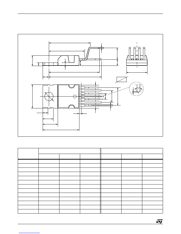
Package Mechanical Data
STV9302A
12/15
7
Package Mechanical Data
Figure 13: 7-pin Heptawatt Package
Table 1: Heptawatt Package
Dim.
mm
inches
Min.
Typ.
Max.
Min.
Typ.
Max.
A
4.8
0.189
C
1.37
0.054
D
2.40
2.80
0.094
0.110
D1
1.20
1.35
0.047
0.053
E
0.35
0.55
0.014
0.022
E1
0.70
0.97
0.028
0.038
F
0.60
0.80
0.024
0.031
G
2.34
2.54
2.74
0.095
0.100
0.105
G1
4.88
5.08
5.28
0.193
0.200
0.205
G2
7.42
7.62
7.82
0.295
0.300
0.307
H2
10.40
0.409
H3
10.05
10.40
0.396
0.409
L
16.70
16.90
17.10
0.657
0.668
0.673
A
L
L1
C
D1
L5
L2
L3
D
E
M1
M
H3
Dia.
L7
L11
L10
L6
H2
F
G
G1
G2
E1
F
E
L9
V4
L4
H2
13/15
STV9302A
Package Mechanical Data
L1
14.92
0.587
L2
21.24
21.54
21.84
0.386
0.848
0.860
L3
22.27
22.52
22.77
0.877
0.891
0.896
L4
1.29
0.051
L5
2.60
2.80
3.00
0.102
0.110
0.118
L6
15.10
15.50
15.80
0.594
0.610
0.622
L7
6.00
6.35
6.60
0.0236
0.250
0.260
L9
0.20
0.008
L10
2.10
2.70
0.082
0.106
L11
4.30
4.80
0.169
0.190
M
2.55
2.80
3.05
0.100
0.110
0.120
M1
4.83
5.08
5.33
0.190
0.200
0.210
V4
40 (Typ.)
Dia.
3.65
3.85
0.144
0.152
Table 1: Heptawatt Package (Continued)
Dim.
mm
inches
Min.
Typ.
Max.
Min.
Typ.
Max.
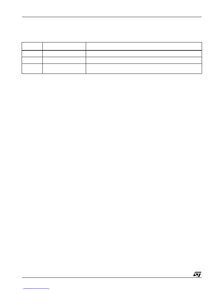
Revision History
STV9302A
14/15
8
Revision History
Table 2: Summary of Modifications
Version
Date
Description
2.0
January 2002
First Issue.
2.1
November 2002
Addition of Stand-by Control information,
Section 8: Revision History
.
2.2
April 2003
Correction to
Section 4.1.1.2: Peak Current
. Creation of new title,
Section
4.3.4: Secondary Breakdown Diagrams
.

15/15
STV9302A
Information furnished is believed to be accurate and reliable. However, STMicroelectronics assumes no responsibility for the
consequences of use of such information nor for any infringement of patents or other rights of third parties which may result from its
use. No license is granted by implication or otherwise under any patent or patent rights of STMicroelectronics. Specifications
mentioned in this publication are subject to change without notice. This publication supersedes and replaces all information previously
supplied. STMicroelectronics products are not authorized for use as critical components in life support devices or systems without
express written approval of STMicroelectronics.
The ST logo is a registered trademark of STMicroelectronics
© 2003 STMicroelectronics - All Rights Reserved
STMicroelectronics GROUP OF COMPANIES
Australia - Brazil - Canada - China - Finland - France - Germany - Hong Kong - India - Israel - Italy - Japan
Malaysia - Malta - Morocco - Singapore - Spain - Sweden - Switzerland - United Kingdom - U.S.A.
www.st.com