Full Text Searchable PDF User Manual

VN210 RF Modem
User Manual

1
Proprietary & Confidential
1. Purpose of document ............................................................................................................... 2
2. Overview of the radio modem hardware ............................................................................. 2
3. Operation of the CDS radio modem ..................................................................................... 5
3.1. Getting started ................................................................................................................... 5
4. RF exposure limit warning ....................................................................................................... 6
5. Compliance statement (part 15.19) ....................................................................................... 6
6. OEM responsibility .................................................................................................................... 6
7. Warning (Part 15.21) ................................................................................................................ 6
8. Revision history ......................................................................................................................... 7
Control Data Systems
Version 1.0
Created: February 1st, 2017
2
Proprietary & Confidential
This document was created in order to provide to the user clear guidelines regarding the
usage of the VN210 RF modem.
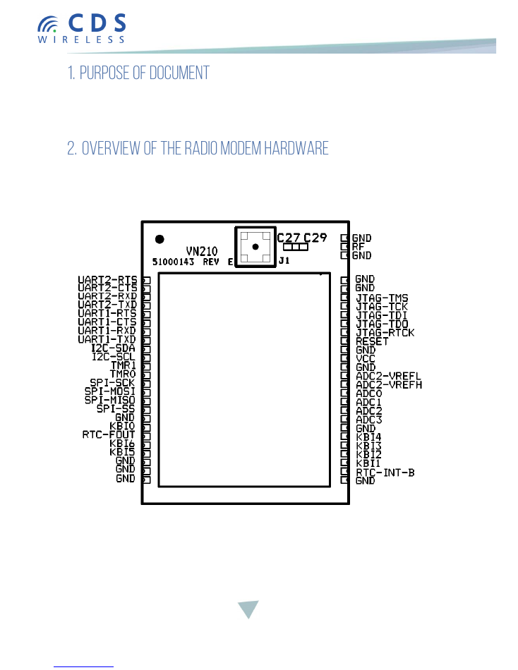
The VN210 radio modem is an 802.15.4 wireless module that allows communication
using a standard asynchronous serial data stream. The pin-out of the VN210 radio
modem is presented in the figure below.
CDS

3
Proprietary & Confidential
No.
Name
Description
Type
Dir
Comments
1
UART2-RTS
UART2 Request to Send
DIG
I
Can be configured as GPIO
2
UART2-CTS
UART2 Clear to Send
DIG
O
Can be configured as GPIO
3
UART2-RXD
UART2 Receive Data
DIG
I
Can be configured as GPIO
4
UART2-TXD
UART2 Transmit Data
DIG
O
Can be configured as GPIO
5
UART1-RTS
UART1 Request to Send
DIG
I
Can be configured as GPIO
6
UART1-CTS
UART1 Clear to Send
DIG
O
Can be configured as GPIO
7
UART1-RXD
UART1 Receive Data
DIG
I
Can be configured as GPIO
8
UART1-TXD
UART1 Transmit Data
DIG
O
Can be configured as GPIO
9
I2C-SDA
I2C bus DATA
DIG
1
I/O
Can be configured as GPIO
10
I2C-SCL
I2C bus CLOCK
DIG
1
I/O
Can be configured as GPIO
11
TMR1
Timer 1 I/O
DIG
I/O
Can be configured as GPIO
12
TMR0
Timer 0 I/O
DIG
I/O
Can be configured as GPIO
13
SPI-SCK
SPI Clock
DIG
O
2
Can be configured as GPIO
14
SPI-MOSI
SPI Data Out
DIG
O
2
Can be configured as GPIO
15
SPI-MISO
SPI Data In
DIG
I
2
Can be configured as GPIO
16
SPI-SS
SPI Slave Select
DIG
O
2
Can be configured as GPIO
17
GND
Ground
N/A
N/A
18
KBI0
RTC clock out enable /
Keyboard interface pin 0
DIG
O
19
RTC-FOUT
32768Hz RTC clock out
DIG
O
20
KBI6
Keyboard interface pin 6
DIG
I/O
Can be configured as GPIO
21
KBI5
Keyboard interface pin 5
DIG
I/O
Can be configured as GPIO
22
GND
Ground
N/A
N/A
23
GND
Ground
N/A
N/A
24
GND
Ground
N/A
N/A
25
GND
Ground
N/A
N/A
26
RTC-INT-B
RTC wake-up interrupt /
DIG
O

4
Proprietary & Confidential
Keyboard interface pin 7
27
KBI1
Keyboard interface pin 1
DIG
I/O
Can be configured as GPIO
28
KBI2
Keyboard interface pin 2
DIG
I/O
Can be configured as GPIO
29
KBI3
Keyboard interface pin 3
DIG
I/O
Can be configured as GPIO
30
KBI4
Keyboard interface pin 4
DIG
I/O
Can be configured as GPIO
31
GND
Ground
N/A
N/A
32
ADC3
ADC pin 3
Analog
I
Can be configured as GPIO
33
ADC2
ADC pin 2
Analog
I
Can be configured as GPIO
34
ADC1
ADC pin 1
Analog
I
Can be configured as GPIO
35
ADC0
ADC pin 0
Analog
I
Can be configured as GPIO
36
ADC2-VREFH
ADC2 reference, high pin
Analog
I
Can be configured as GPIO
37
ADC2-VREFL
ADC2 reference, low pin
Analog
I
Can be configured as GPIO
38
GND
Ground
N/A
N/A
39
VCC
Supply voltage
N/A
N/A
40
GND
Ground
N/A
N/A
41
RESET
RESET pin
DIG
I
42
JTAG-RTCK
JTAG Return Clock /
ADC pin 7
DIG
O
Can be configured as GPIO
Can be configured as Analog In
43
JTAG-TDO
JTAG Test Data Output
DIG
O
Can be configured as GPIO
44
JTAG-TDI
JTAG Test Data Input
DIG
I
Can be configured as GPIO
45
JTAG-TCK
JTAG Test Data Input
DIG
I
Can be configured as GPIO
46
JTAG-TMS
JTAG Test Mode Select
DIG
I
Can be configured as GPIO
47
GND
Ground
N/A
N/A
48
GND
Ground
N/A
N/A
49
GND
Ground
N/A
N/A
50
RF
RF pin
Analog
I/O
52
GND
Ground
N/A
N/A
5
Proprietary & Confidential
Notes:
1.)
Open collector pin if configured as I2C port
2.)
Signal Dir valid if module is configured as SPI Master
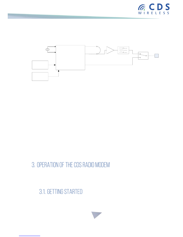
MC13224
SoC
Ceramic LPF
MBC13720
Power
Amplifier
CEL
uPG2214T/R
Switch
24 MHz
Crystal
512KB
Flash memory
BALUN
Network
Antenna connector
MMCX
32768Hz RTC
Power is supplied to the modem through pins 38, 39 and 40.
Pin 39 must be supplied with 2.7 to 3.3 Volts and powers the digital and RF functional
entities of the modem. The modem has internal filtering circuitry to smooth out the
supply voltage but it has no onboard regulators.
All of the remaining pins of the modem are I/O lines of the processor, except for pin 50,
which is the RF I/O port.
The voltage on any of the I/O lines should never exceed VCC+0.3 V.
Pins 1 to 4 are attached to UART 2. Pins 5 to 8 are attached to UART1. If connecting to
the serial port of a PC, a level-shifting transceiver must be employed in order to provide
the appropriate voltage levels on the RX and TX lines.
Communication with the VN210 radio modem happens through serial port 1. The baud-
rate is set to be 115200, 8N1.
Open a terminal software on a serial port with the above settings and connect to the RF
modem. Upon power up, the terminal will display a list of the available commands.
6
Proprietary & Confidential
To comply with FCC’s RF exposure limits for general population / uncontrolled exposure,
the antenna(s) used for this transmitter must be installed to provide a separation
distance of at least 20cm from all persons and must not be co-located or operating in
conjunction with any other antenna or transmitter.
This Device complies with Part 15 of the FCC Rules. Operation is subject to the following
two conditions:
1.
This device may not cause harmful interference, and
2.
This device must accept any interference received, including interference that
may cause undesired operation.
The VN210 RF Module has been certified per FCC Part 15 rules for integration into
products without further testing or certification. To fulfill the FCC certification
requirements the OEM of the VN210 RF Module must ensure that the information
provided on the VN210 RF Module label is placed on the outside of the final product.
The VN210 RF Module is labeled with its own FCC ID Number. If the FCC ID is not visible
when the module is installed inside another device, then the outside of the device into
which the module is installed must also display a label referring to the enclosed module.
This exterior label can use wording such as the following:
“Contains Transmitter Module FCC ID: 2AKZ5-CDSVN210ISA” or
“Contains FCC ID: 2AKZ5-CDSVN210ISA”
Only the approved antennas, which have been certified with this module should be
used. The approved antennas are:
ANT-2.4-CW-RCT-RP Linx Technologies (2.2dBi)
ANT-N-5 Mini-Box (5.5 dBi)
FS1-F9915KB Yokogawa (2.0 dBi)
Changes or modifications not expressly approved by the party responsible for
compliance could void the user’s authority to operate the equipment.

7
Proprietary & Confidential
Date
Revision
Description
Author
02/01/201 1.0
Document Creation
Adrian Vatamanu