Full Text Searchable PDF User Manual

R·I·T
Title: ASML Stepper
Semiconductor & Microsystems
Fabrication Laboratory
Revision: B Rev Date: 12/21/2010
Approved by:
/ / / /
Process Engineer Equipment Engineer
RIT SMFL
Page 1 of 11
1
SCOPE
The purpose of this document is to detail the use of the ASML PAS 5500 Stepper. All users are expected
to have read and understood this document. It is not a substitute for in-person training on the system and
is not sufficient to qualify a user on the system. Failure to follow guidelines in this document may result
in loss of privileges.
2
REFERENCE DOCUMENTS
Batch Control PAS 5500 Training Module
Reticle Design Manual
PAS 5500 User Guide
PAS 5500 Job Definition
PAS Global Alignment Strategies
PAS 5500 Steppers up to and including /300 Stepper Introduction
3
DEFINITIONS
n/a
4
TOOLS AND MATERIALS
4.1
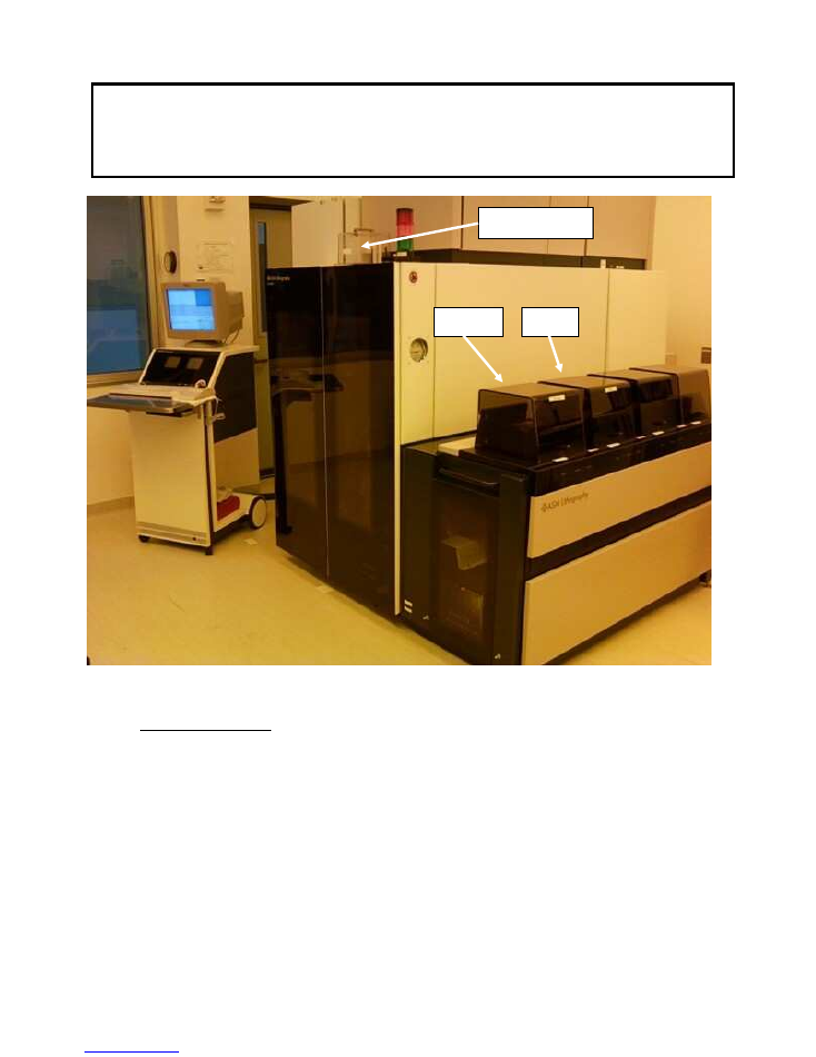
General Description - The ASML PAS 5500/200 is a 5x reduction, i-line stepper set up for
exposure of 6 inch wafers using 6 inch reticles. The system has 350nm resolution with a
0.48-0.60 variable numerical aperture. The maximum field size on the wafer is 22x22mm.
Overlay capability is better than 50nm. All lithography levels for a particular design are
included in a single stepper job.
R·I·T
Title: ASML Stepper
Semiconductor & Microsystems
Fabrication Laboratory
Revision: B Rev Date: 12/21/2010
RIT SMFL
Page 2 of 11
←
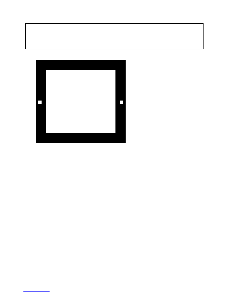
Reticle Pre-Alignment Marks
←
Reticle Barcode
←
Reticle Alignment Marks
4.2
Reticle Bar Code – The reticle barcode is read as the reticle is removed from the reticle
carrier. Reticle bar code information is specified in the stepper job.
4.3
Reticle Pre-Alignment Marks – Two Pre-alignment Marks are located 135.5mm apart near
the corners of the reticle. They are used to pre-align the reticle to the reticle table.
4.4
Reticle Alignment Marks - Two Reticle Alignment Marks, M1 and M2, are located 139mm
apart near the left and right edges of the reticle. After the reticle is pre-aligned on the reticle
table, the Reticle Alignment Marks are aligned to the permanent fiducial marks F1 and F2,
located on the fiducial plate on the wafer table.
4.5
Wafer Zero Level – The ASML Stepper utilizes zero level marks that are patterned and
etched into the wafer before any other steps. An etch depth of 1200A +/- 10% allows the
stepper to recognize the marks. It is possible to pattern the zero level at the same time as the
first level, but overlay accuracy will be reduced since the first level is not aligned to the zero
level. This is because the zero level is defined by a separate reticle.
4.6
Wafer Global Alignment - The wafer alignment marks W1, W2, etc, are exposed on the
zero layer and etched into the wafer. Two of these marks are sufficient but up to 25 may be
used on a single wafer. If more than two marks are used, the stepper will find a best
alignment and expose all die using the same settings. The stepper uses through the lens
alignment of the wafer and the reticle.
*
*
||||
||||
||||
|||
R
IT
R
IT

R·I·T
Title: ASML Stepper
Semiconductor & Microsystems
Fabrication Laboratory
Revision: B Rev Date: 12/21/2010
RIT SMFL
Page 3 of 11
4.7
Wafer Field by Field Alignment – This method uses marks that are part of the CAD data
for each mask layer; they are not exposed individually. These marks may be placed in the
scribe lanes. Field by field alignment takes longer than global alignment because each die is
aligned.
4.8
Standard Jobs – Several standard jobs are available for use with the Standard Reticle
Templates. This allows a user to process wafers without having to develop a new stepper
job. These jobs should not be changed but may be copied and saved as new jobs.
5
SAFETY PRECAUTIONS
5.1
Hazards to the Operator
5.1.1
The ASML uses ultraviolet light as well as lasers, and should only be operated with
all of the covers closed. Safety glasses should be worn at all times.
5.1.2 The ASML stepper had mechanical hazards. Do not operate with open covers and
do not open any covers during operation.
5.2
Hazards to the Tool
5.2.1
Never open or service the wafer stage since serious damage to the tool can occur.
5.2.2
Never manually remove stuck wafers from the system. Please contact the tool
technician.
5.2.3
Reticle changing should only be done by a certified user. Use care not to touch the
surface of the reticle. If alignment marks become obscured, the stepper will not be
able to find them.
5.2.4
Do not remove the Combi reticle from the SMIF pod. It is fragile and expensive to
replace.
5.2.5
Wafers must have clean backs. This will keep the stage clean and prevent errors.
5.2.6
Do not remove a carrier that is not fully raised.
R·I·T
Title: ASML Stepper
Semiconductor & Microsystems
Fabrication Laboratory
Revision: B Rev Date: 12/21/2010
RIT SMFL
Page 4 of 11
6
INSTRUCTIONS
6.1
Starting the System
6.1.1
Swipe the tool in on the Card Swipe System.
6.1.2
Verify that the computer is on.
6.1.3
Make sure that the computer is on the Main Menu, if not select 0 Exit. Do not exit
from the Main Menu.
Unload
Load
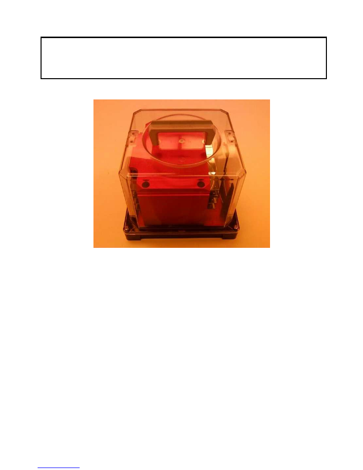
Reticle Changer
R·I·T
Title: ASML Stepper
Semiconductor & Microsystems
Fabrication Laboratory
Revision: B Rev Date: 12/21/2010
RIT SMFL
Page 5 of 11
6.2
Loading the Reticles
6.2.1 To remove the reticle box from the machine, under select Mat Hdl from the top of
the screen and then 3 – Exchange Reticle Box. Click the Unlock button in the
middle of the screen to unlock the reticle box.
6.2.2 Remove the box by lifting straight up 2 cm, tilting the front up and moving it away
from the stepper at a 45 degree angle. Always support the reticle box on the bottom
to prevent reticles from falling out.
6.2.3 Carefully open the reticle box. The clear top is released from the base by sliding
the 4 clamps underneath the base. Load the reticles chrome side down with the pre-
alignment stars facing out. Never touch the surface of a reticle. Close the reticle
box and make sure it is secured before lifting. Do not remove the Combi Reticle
from the top slot.
6.2.4 To load the reticle box, lower it straight down without tilting it. The open side of
the internal cassette should be towards the stepper.
6.2.5 Select the Read 1 button to read the barcodes and display the reticle IDs.

R·I·T
Title: ASML Stepper
Semiconductor & Microsystems
Fabrication Laboratory
Revision: B Rev Date: 12/21/2010
RIT SMFL
Page 6 of 11
6.2.6 If your reticles do not have bar codes, use the Specify button to enter reticle IDs
and then the Apply button to confirm. This will have to be done each time the
reticles are loaded into the machine.
6.2.7 When finished, the reticle box should be stored on the stepper.
6.2.8 Press Cancel and Exit back to the Main Menu.
6.3
Loading Wafers
6.3.1 Lift the cover to the loader and place the cassette of wafers on the stage. Make sure
that the cassette is properly seated.
6.3.2 Place an empty cassette on the receiver. All 4 stations should have a cassette.
6.4
Defining a Batch and Running a Stepper Job
6.4.1 From the Main Menu, select 2- Batch Control and 1 – Define Batch.
6.4.2 The Batch ID is the name that you use to identify your wafers.
6.4.3 The Job Name is the name of the stepper job that you want to use. Click the Select
button, scroll down, select the job and Accept at the top of the screen. Writing a
stepper job is detailed in a separate document.
6.4.4 Click on the line to the right of Layer ID. Select the Layer Number that you want
to expose when the box comes up. Layer number zero is used for exposing the
alignment marks onto the wafer. See attachments for more information on the zero
level.
6.4.5 The Control Mode may be set to W or C. A setting of C will expose all of the
wafers in the cassette. A setting of W will only expose the number of wafers that
you specify.
6.4.6 The Batch Size is the number of wafers or cassettes that you want to expose.
6.4.7 Under Batch Type select P for production. F will allow you to do a focus
meander, E will allow you to do an energy meander and M will allow you to do a
matrix.

R·I·T
Title: ASML Stepper
Semiconductor & Microsystems
Fabrication Laboratory
Revision: B Rev Date: 12/21/2010
RIT SMFL
Page 7 of 11
6.4.8 Under Process Data you may adjust exposure energy, focus and tilt settings. The
minimum energy is 40mJ/cm
2
. Under Illumination Mode select either
conventional or annular. Numerical aperture and sigma may be specified. After
changing any of these values you must select the Apply button for the changes to
take effect.
6.4.9 The Clear button at the bottom of the screen will clear all of the entries and allow
you to start over.
6.4.10 The Run button will start the batch. Wafers will automatically load, align, expose
and unload.
6.5
Unloading Wafers
6.5.1
Lift the cover on the output cassette and remove the wafers. Do not remove a carrier
that is not fully raised.
6.5.2 Place the empty cassette back on the tool. All 4 stations should have a cassette.
6.6
Unloading Reticles
6.6.1 To remove the reticle box from the machine, under Main Menu, select Mat Hdl
from the top of the screen and then 3 – Exchange Reticle Box. Click the Unlock
button in the middle of the screen to unlock the reticle box.
6.6.2 Remove the box by lifting straight up 2 cm, tilting the front up and moving it away
from the stepper at a 45 degree angle. Always support the reticle box on the bottom
to prevent reticles from falling out.
6.6.3 Carefully open the reticle box. Unload the reticles. Never touch the surface of a
reticle. Close the reticle box and make sure it is secured before lifting.
6.6.4 Replace the reticle box on the stepper by lowering it straight down without tilting it.
The open side of the internal cassette should be towards the stepper. The reticle
box should be stored on the stepper when finished.
6.6.5 Exit back to the Main Menu.

R·I·T
Title: ASML Stepper
Semiconductor & Microsystems
Fabrication Laboratory
Revision: B Rev Date: 12/21/2010
RIT SMFL
Page 8 of 11
6.7
Resetting the System
6.7.1 To remove all wafers from the machine, select Batch Control from the Main
Menu, select Mat Hdl from the top of the screen and then 2 – Remove Wafers
from Machine. Never manually remove stuck wafers from the machine.
6.8
Errors during Run
6.8.1
If any errors occur contact the equipment engineer.
6.9
Introducing a Layer Shift
6.9.1 Select Process Data in your stepper job to enter a layer shift in microns. See
Section 6.8 of the ASML PASS 5500 Job Creation Manual.
7
APPROPRIATE USES OF THE TOOL
7.1
No backside coated wafers, only wafers with clean backs may be processed in this tool.
7.2
No polyimide or SU8 may be processed in this tool.
8
ATTACHMENTS
8.1
Dose to Clear Test (Exposure Matrix)
8.1.1
This test is done with or without a mask and the full field is exposed.
8.1.2
From the Main Menu select 6-Test Manager.
8.1.3
Select 1-Run Test.
8.1.4
Move to the top of the directory by clicking Up.
8.1.5
Select Illumination System.
8.1.6
Select Performance Tests.
8.1.7
Select Resist Uniformity.
8.1.8
Select Accept at the top of the screen.

R·I·T
Title: ASML Stepper
Semiconductor & Microsystems
Fabrication Laboratory
Revision: B Rev Date: 12/21/2010
RIT SMFL
Page 9 of 11
8.1.9
Input the Nominal Energy, the Energy Increment and the Window Size. Be sure
to hit return after each entry.
8.1.10
Select Accept.
8.1.11
One wafer will be exposed with the nominal exposure in the center of the wafer. The
remaining exposures will be divided up above and below this. When the wafer is
finished, a report will come up and show the exposure pattern.
8.1.12
When finished select Exit twice to return to the Main Menu.
8.1.13 A dose to clear test can also be done in the screen used to define a batch.
8.2
FEM (Focus/ Exposure Matrix)
8.2.1 From the Main Menu select 6-Test Manage.
8.2.2 Select 1-Run Test.
8.2.3 Move to the top of the directory by clicking Up.
8.2.4 Select Projection Systems.
8.2.5 Select FEM Developer/Customer.
8.2.6 Select Accept at the top of the screen.
8.2.7 Input desired values for matrix size, energy, increment, focus and the number of die
to be exposed. Each die is a complete focus/ exposure matrix.
8.2.8 Select Accept.
8.2.9 When finished select Exit twice to return to the Main Menu.
8.2.10 A Focus/Exposure test can also be done in the screen used to define a batch.
8.3
Running RIT Daily
8.3.1 From the Main Menu select 6-Test Manager.
8.3.2 At the top of the dialog screen select CMD HDL.
8.3.3 From this screen select 8-Contamination and Temperature Control.

R·I·T
Title: ASML Stepper
Semiconductor & Microsystems
Fabrication Laboratory
Revision: B Rev Date: 12/21/2010
RIT SMFL
Page 10 of 11
8.3.4 Select 2-Sensor Module Commands.
8.3.5 Select 4-Monitor All Sensor Values.
8.3.6 Ensure that the Lens Temperature is 22.01C (+/- 0.02C).
8.3.7 Select Cancel at the top of the screen.
8.3.8 Select Exit 3 times to return to the Test Manager menu.
8.3.9 Select 3 - Run Test Que.
8.3.10 Select Select.
8.3.11 Scroll down until you see daily RIT. Characters are case sensitive.
8.3.12 Select Accept at the top of the screen.
8.3.13 Select Accept again and the test will run.
8.3.14 Select Exit twice to return to the Main Menu.
8.4
Procedure for Creating a Zero Level
8.4.1 Load the Combi Reticle.
8.4.2 Select your stepper job.
8.4.3 Select Layer ID.
8.4.4 Select Zero Layer to expose your marks.
8.4.5 Develop and bake the resist.
8.4.6 Plasma etch the zero level marks with the Drytek Quad using the ZEROETCH
recipe. The marks should be 1200Å +/- 10%.
8.4.7 Strip the photoresist.
R·I·T
Title: ASML Stepper
Semiconductor & Microsystems
Fabrication Laboratory
Revision: B Rev Date: 12/21/2010
RIT SMFL
Page 11 of 11
REVISION RECORD
Summary of Changes
Originator
Rev/Date
Original Issue
Sean O’Brien A-07/20/2010
Clarified some of the instructions
Sean O’Brien B-12/21/2010